Process Characteristics of PCB Reflow Oven
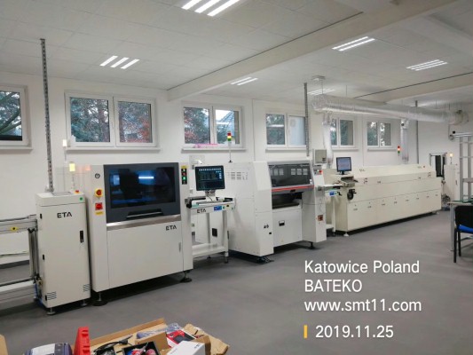
I.C.T SMT manufacturer provide best price SMT reflow oven, SMD reflow oven, PCB reflow oven, with 6 zones, 8 zones, 10 zones and 12 zones.
Lead-free wave soldering and lead-free reflow oven are necessary welding equipment for the production and welding of electronic products. Lead-free wave soldering is used to solder active plug-in electronic components. Device, lead-free reflow is also a part of the SMT production process. The following share the characteristics of lead-free reflow oven compared with lead-free wave soldering.
1. The lead-free reflow oven process is not like the lead-free wave soldering. The components are directly immersed in the molten solder, so the components are subject to small thermal shock. However, due to different heating methods for lead-free reflow, larger thermal stresses are sometimes applied to components;
2. The lead-free SMT reflow oven process only needs to apply solder on the pads, and can control the amount of solder applied, avoiding the occurrence of welding defects such as false soldering and continuous soldering, so the soldering quality is good and the reliability is high;
3. The lead-free PCB reflow oven process has a self-positioning effect. When the component placement position is deviated, due to the surface tension of the molten solder, when all solder ends or pins are wetted at the same time as the corresponding pads, the surface is The phenomenon of being automatically pulled back to the approximate target position under the action of tension;
4. No solder will be mixed into the solder in the lead-free reflow oven process. When using a solder paste, the solder composition can be correctly guaranteed;
5. The lead-free reflow oven process can use local heating heat sources, so that different soldering processes can be used for soldering on the same circuit board;
6. The lead-free reflow oven process is simpler than the lead-free wave soldering process, and the work of repairing the board is small, thereby saving manpower, power and materials.
❙ PCB Reflow Oven Video